PCIe Switch 问题点

系列文章目录
文章目录
- 系列文章目录
- 完善
- PCIe Retimer Overview Document Outline
- Switch 维度
- BroadCom
- MicroChip
- Asmedia 祥硕
- Cyan
- 其他
完善
- Functional block diagram,功能框图
- Key Features and Benefits,主要功能和优点
- Fabric 链路
- Multi-root
PCIe Retimer Overview Document Outline
KB90xx (Regli™) PCIe Retimer Overview Document Outline
-
Introduction
- Overview of KB90xx (Regli™) PCIe Retimer family
- Purpose and target applications
-
Kandou’s Unique Chiplet Approach
- Single-silicon development for multiple products (x16, x8, x4 retimers)
- Integration of Glasswing interface for low-power, low-latency chiplet communication
-
KB900x Product Overview
- Key Features:
- Compliance with PCIe Gen5/CXL 2.0 standards
- Low latency (~10ns), insertion loss compensation (up to 36dB@16GHz)
- Dynamic lane skew compensation, automatic offset calibration
- Support for L1PM substates, on-chip diagnostics (eye scope, BER monitors, logic analyzer)
- Voltage Flexibility:
- PWR_1 (VDD_IO): 1.8V
- PWR_2 (VDD_CORE): 0.9V
- PWR_12 (VDD_PHY): 1.8V (Regular) or 1.2V/1.5V (Power Saving Mode)
- Packaging Options:
- KB9003 (x16): 354-ball BGA (8.9mm×22.8mm)
- KB9002 (x8): 332-ball BGA (8.5mm×13.4mm)
- KB9001 (x4): 146-ball BGA (5.5mm×10mm)
- Key Features:
-
KB900x Product Family Comparison (NDA Required)
Feature KB9003 KB9002 KB9001 PCIe Lanes 16 (Bidir) 8 (Bidir) 4 (Bidir) CXL Support CXL 1.0/2.0 CXL 1.0/2.0 CXL 1.0/2.0 Insertion Loss Comp. Rx: 36dB@16GHz Same as KB9003 Same as KB9003 Power Consumption 14.7W 7.4W 3.7W Availability ES: Now CS: May 2024 CS: Q1 2025 -
KB900x Functional Block Diagram
- Integration of AC coupling capacitors (220nF)
- MCU with EEPROM/SPI Flash boot options
- 100MHz HCSL clock source for PCIe reference clocks
-
KB900x Key Features & Benefits
- Co-design compatibility with Astera Labs
- Dynamic channel loss compensation (up to 36dB)
- Secure platform boot support
- Integrated logic analyzer for real-time debugging
- Power-saving modes (1.2V/1.5V supply)
-
KB900x Software Overview
- Besso GUI for advanced debugging features
- Remote diagnostics capabilities
-
KB900x Advanced Debug Features
- Eye Scope & BER Monitors: Analyze signal integrity and bit error rates
- RTSSM Analyzer: Track state transitions across all lanes
- Logic Analyzer: Trigger on signals (rising/falling edges) for upstream/downstream debug
- Link Training Widget: Visualize PCIe Gen1-Gen5 link speeds and states
-
KB900x Link Training States
- States: INACTIVE (gray), FAILED (red), ACTIVE (blue), PASSED (green)
- Components: Detect, Polling, Configuration, Recovery, Loopback, L0 (Operational)
-
KB9003 CEM (x16 Lane) Riser Card
- Evaluation board for KB9003
- USB-connected PC control via Besso app
-
Retimer Use Cases
- Genoa-based interoperability testing
- Ethernet SmartNIC (ConnectX) integration
- MCIO AEC test configurations
-
PCIe TSSM Block Diagram
- Illustrates link training states (LTSSM) and protocol awareness
-
KB900x Debugging Tools
- Firmware update and version display
- Temperature sensor monitoring
- Register dump and soft/hard MCU reset
- Logic analyzer trigger conditions (e.g., pl_ltssm = 0x10 for L0 state)
-
Conclusion & Support
- Global technical assistance from Kandou’s AE/FAE teams
- Accelerated time-to-market through co-design and prototyping support
附录图表说明
- KB900x Functional Block Diagram: 展示芯片功能模块(AC电容、MCU、时钟源)。
- KB900x RTSSM Analyzer: 实时状态转换监控界面截图。
- KB900x Logic Analyzer: 触发条件配置与信号采样界面示例。
Switch 维度
- Part Number, 部件编号
- PCI-Sig Base Spec, PCI-SIG 规范版本
- Lanes,通道数
- Port Count,端口数量
- Product Brief,产品简介
- ACS/ARI,访问控制服务/高级可扩展接口
- DMA,直接内存访问
- Dual/Multi Cast,单播/多播
- Latency,延迟
- Multi-Root/Multi-Host,多根/多主机
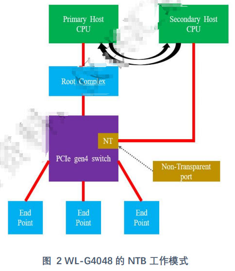
- Non-Transparency,非透明性
- Packaging Size,封装尺寸
- Power Typ. ,典型功耗
- Read Pacing,读取速率控制
- Virtual Channels,虚拟通道
BroadCom
ExpressFabric Switch and Retimer Solutions
博通PCIe Switch-学习笔记
MicroChip
Switchtec™ PCIe® Switches
Asmedia 祥硕
PCIe Switch
Cyan
其他
NVMe All Flash Array (AFA) systems
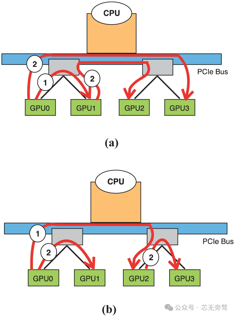
青芯说,国内现在他们的 PCIe4 Switch 用的最多的是 Storage RAID 卡(下行多个x4,上行一般是x8或者x16),和 GPU的一卡双芯(上行X16,两个下行X16)
全球PCIe交换芯片(PCIe Switch)核心厂商包括Broadcom、Microchip和Texas Instruments等,前三大厂商占有全球大约80%的份额。亚太是最大的市场,占有大约75%的份额。产品类型而言,PCIe 3.0是最大的细分,占有大约47%的份额。就下游来说,企业级是最大的下游领域,占有约45%的份额。
AI产业笔记(二):存算一体和PCIe SW芯片
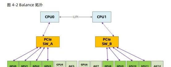
- Balance 拓扑:每个CPU下连接1个PCIe SW芯片,每个PCIe SW芯片最多可以连接5张GPU。远端GPU P2P通信受限于CPU间的UPI通信瓶颈,比较适用于VDI、公有云、AI训练等场景,属目前市场主流拓扑。
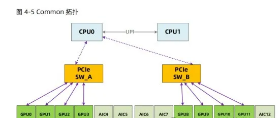
- Common 拓扑:CPU0下连接2个PCIe SW芯片,每个PCIe SW芯片连接4张GPU。远端GPU通信无需跨CPU通信,GPU P2P吞吐量高。适合CPU参与较多任务的P2P通信密集训练算法模型,如Resnet 101/50。
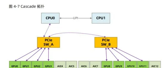
- Cascade 拓扑:CPU0 直连1个 PCIe SW芯片,此PCIe SW芯片与另一个PCIe SW芯片互联,每个PCIe SW芯片下面连接 4 张 GPU。Switch 芯片互联提供最强的 GPU P2P 通信,但CPU到GPU吞吐量小。适合CPU参与较少任务的P2P参数密集型训练算法模型如VGG-16。
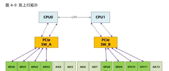
- 双上行拓扑:每个CPU下连接一个PCIe SW芯片,每个PCIe SW芯片连接4张GPU。CPU利用率最大化,提供最大上行链路带宽(2个x16的速率),但远端GPU P2P通信受限于CPU间的UPI通信瓶颈,适用于VDI、公有云、AI训练等场景。